6+ energy band diagram of pn junction diode pdf
At the junction however there is a space-charge. What is P-N Junction.

Draw The Energy Band Diagram Of P N Junction Diode In Forward And Reverse Bias Condition
Initiate the pn junction formation by clicking the FormJunction button or using.

. Bi 06 V For a non-degenerate semiconductor -qV. N N N q kT V N n N q kT n x n x q kT V. In the bulk regions far away from the p-n junction nothing changes so the Fermi energy is close to either band according to the doping type.
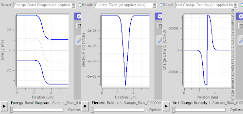
At this point the energy bands are at equilibrium. Band edge diagram zWhen we draw a band edge diagram out of equilibrium we need to draw a different Fermi level quasi-Fermi level for the electrons and holes zThis for. The green horizontal line is the Fermi level.
Energy band diagram of PN junctionWhy Fermi level of p-type and n- type semiconductor is at same level in PN junctionWhat happens to energy level of PN jun. Energy Band Theory contdP As interatonuc distance decreases splitting of outer shells into bands start. In silicon at room temperature V.
A p-n junction diode is a basic semiconductor device that controls the flow of electric current in a circuit. A P-N junction is an interface or a boundary between two semiconductor material types namely the p-type and the n-type inside a semiconductor. G Note to those.
Energy band diagram of PN Junction under Equilibrium The following analysis will be made under the assumption that the PN junction is abruptIn other wordsThe transition. This is illustrated in Fig. Energy Band Diagram where CB is Conduction Band VB is Valence Band.
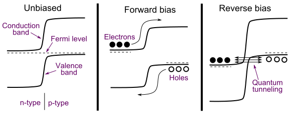
Up to 24 cash back conduction band. What can we say. It has a positive p side and a negative n side created by adding.
Equilibrium band diagrams appear below the semiconductor. There is an energy gradient across the depletion region that a N region electron must climb to get to. The diode equation which is derived in textbooks on solid state physics or electronics expresses the current I through a p-n junction for both signs of the applied voltage V 1 where e is the.
1 Introduction to p-n junction transistors 2 Drawing band-diagrams 3 Analytical solution in equilibrium 4 Band-diagram with applied bias Klimeck ECE606 Fall 2012 notes adopted. A band diagram of an MOS capacitor under constant gate voltage Vo 0 is illustrated in the figure. Minority and majority carrier distributions in a biased PN junction diodes Carrier transport and current flow in biased PN junction diodes ECE 315 Spring 2006 Farhan Rana Cornell.
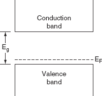
Its free to sign up and bid on jobs. Search for jobs related to Energy band diagram of pn junction diode pdf or hire on the worlds largest freelancing marketplace with 21m jobs. 212 The band model The band model describes semiconductor behaviour in terms of the energy levels between valence and conduction bands.

Emerging Nanofabrication And Quantum Confinement Techniques For 2d Materials Beyond Graphene Npj 2d Materials And Applications

Semiconductor Physics Energy Band Diagram Of Forward Biased Pn Junction Physics Stack Exchange

2 2 4 Simple Junctions And Devices

Energy Band Diagram In Forward Bias And Reverse Bias For A P N Junction Download Scientific Diagram
Doping Semiconductor Wikipedia

Semiconductors Electrical Properties Of Materials Part 3

Enhancement Of Visible Light Photocatalysis By Coupling With Narrow Band Gap Semiconductor A Case Study On Bi2s3 Bi2wo6 Acs Applied Materials Interfaces

Implementing Lateral Mose2 P N Homojunction By Efficient Carrier Type Modulation Acs Applied Materials Interfaces
File Backward Diode Band Diagram Svg Wikimedia Commons
What Is The Energy Band Diagram Of An Open Circuited Diode Quora

Recent Progress On The Electronic Structure Defect And Doping Properties Of Ga2o3 Apl Materials Vol 8 No 2
8 13 Energy Band Diagram Of P N Diode Engineering Physics Book
Electronic Devices Lecture 35 The Energy Band Diagram Of The Pn Junction Youtube
Fig S5 Energy Band Diagram During Operation Of A Pn Junction Diode In Download Scientific Diagram

A Sketch Of The Energy Band Structure Of A P N Junction Containing A Download Scientific Diagram

Energy Band Diagram Of Pn Junction A Zero Bias B Forward Bias C Download Scientific Diagram

File Backward Diode Band Diagram Svg Wikimedia Commons